- Courses
- GS Full Course 1 Year
- GS Full Course 2 Year
- GS Full Course 3 Year
- GS Full Course Till Selection
- Online Program
- GS Recorded Course
- NCERT (Recorded 500+ Hours)
- Polity Recorded Course
- Geography Recorded Course
- Economy Recorded Course
- AMAC Recorded Course
- Modern India, Post Independence & World History
- Environment Recoded Course
- Governance Recoded Course
- Science & Tech. Recoded Course
- International Relations and Internal Security Recorded Course
- Disaster Management Module Course
- Ethics Recoded Course
- Essay Recoded Course
- Current Affairs Recoded Course
- CSAT
- 5 LAYERED ARJUNA Mentorship
- Public Administration Optional
- ABOUT US
- OUR TOPPERS
- TEST SERIES
- FREE STUDY MATERIAL
- VIDEOS
- CONTACT US
Programme for Development of Semiconductors and Display Manufacturing Ecosystem
Programme for Development of Semiconductors and Display Manufacturing Ecosystem
09-09-2024
Program Approval:
- Objective: Enhance India’s semiconductor and display manufacturing industry.
- Budget: ₹76k crore (>10 billion USD) allocated.
Key Modifications:
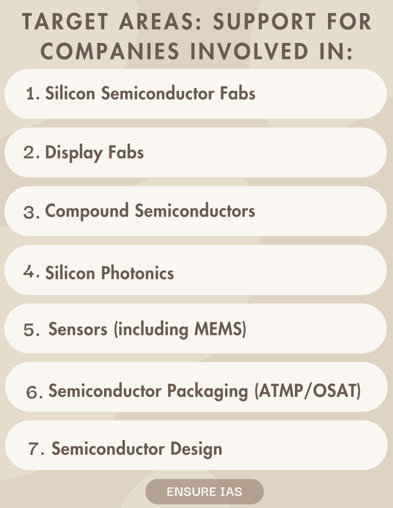
- Financial Support:
- Semiconductor Fabs: 50% of project cost covered.
- Display Fabs: 50% of project cost covered.
- Other Facilities: 50% of capital expenditure supported for compound semiconductors, silicon photonics, sensors, and semiconductor packaging facilities.
Schemes Under the Program:
-
Semiconductor and Display Fabs:
- Support: 50% of project cost for eligible projects.
- Goal: Establish at least two new semiconductors and two display fabs.
- Support Structure: Collaboration with state governments to build necessary infrastructure.
-
Compound Semiconductors and Related Facilities:
- Support: 50% of capital expenditure.
- Goal: Set up at least 20 new units for compound semiconductors and semiconductor packaging.
-
Semiconductor Design:
- Incentives:
- Up to 50% of eligible design expenditure.
- Product deployment incentives ranging from 6% to 4% on net sales for five years.
- Target: Support 100 domestic design companies and help 20 companies achieve over ₹1500 crore in turnover.
- Incentives:
-
Semi-Conductor Laboratory (SCL):
- Action: Modernize and commercialize SCL in Mohali.
- Plan: Explore joint ventures with commercial partners for modernization.
India Semiconductor Mission:
- Purpose: Guide long-term strategies for developing the semiconductor and display ecosystem.
- Leadership: Led by global experts.
- Role: Manage and implement the semiconductor and display fab schemes efficiently.
Significance of Modified Programme for Development of Semiconductors and display manufacturing ecosystem
- Boosts Local Manufacturing: Encourages domestic production of semiconductors and display technologies, reducing reliance on imports. Targets include establishing at least 2 semiconductor and 2 display fabs (Government of India, 2022).
- Attracts Investment: Offers 50% financial support for setting up fabs, attracting significant foreign and domestic investment. Expected to channel ₹76,000 crore into the sector, supporting economic growth (NITI Aayog, 2023).
- Enhances Technology Capabilities: Supports advanced technology areas like compound semiconductors and silicon photonics. Aims to set up 20 new units, boosting India’s position in cutting-edge tech (Ministry of Electronics and IT, 2023).
- Promotes Domestic Design: Provides up to 50% design expenditure incentives for semiconductor design companies, aiding 100 firms. Supports growth in ICs, chipsets, and SoCs, fostering innovation (Design Linked Incentive Scheme, 2023).
- Modernizes Existing Infrastructure: Focuses on upgrading the Semi-Conductor Laboratory (SCL) in Mohali. Plans include joint ventures for modernization, enhancing existing facilities and capabilities (Union Cabinet, 2023).

Must Check: Best IAS Coaching In Delhi
UPSC Prelims Result 2024 Out: Expected Cut Off & Other Details, UPSC Prelims 2024 Answer with Explanation, Daily Prelims Quiz, Daily Current Affairs, MONTHLY CURRENT AFFAIRS TOTAL (CAT) MAGAZINE, Best IAS Coaching Institute in Karol Bagh, Best IAS Coaching Institute in Delhi, Daily Mains Question Answer Practice, ENSURE IAS UPSC Toppers, UPSC Toppers Marksheet, Previous Year Interview Questions, UPSC Syllabus
Donald Trump's 'One Big Beautiful Bill Act of 2025' (OBBBA)

Tyre Particles: How EVs are a climate solution with pollution problem

New Damselfly Species Discovered: Caliphaea Sinuofurcata
Karol Bagh Metro Pillar No. 112, Above Domino's, 22B, First Floor, New Delhi - 110060
Very Important Instruction For Any Issue, Student Must Produce His/Her Fee Receipt. Without Fee Receipt, It Will Not Be Possible To Track Your Details. If You Have Been Given Any Special Consideration, You Must Keep That In Writing And Produce In Case Of Conflict.
Copyright © 2024-2026 ENSURE IAS. All rights reserved.