- Courses
- GS Full Course 1 Year
- GS Full Course 2 Year
- GS Full Course 3 Year
- GS Full Course Till Selection
- Online Program
- GS Recorded Course
- NCERT (Recorded 500+ Hours)
- Polity Recorded Course
- Geography Recorded Course
- Economy Recorded Course
- AMAC Recorded Course
- Modern India, Post Independence & World History
- Environment Recoded Course
- Governance Recoded Course
- Science & Tech. Recoded Course
- International Relations and Internal Security Recorded Course
- Disaster Management Module Course
- Ethics Recoded Course
- Essay Recoded Course
- Current Affairs Recoded Course
- CSAT
- 5 LAYERED ARJUNA Mentorship
- Public Administration Optional
- ABOUT US
- OUR TOPPERS
- TEST SERIES
- FREE STUDY MATERIAL
- VIDEOS
- CONTACT US
Miniature Laser Grown on Silicon Chip
Miniature Laser Grown on Silicon Chip
17-04-2025
- Recently, Scientists from the US and Europe have successfully grown miniature lasers directly on silicon wafers.
- This marks a major progress in silicon photonics, a technology that uses light (photons) instead of electricity (electrons) to transmit information on chips.
What is Silicon Photonics?
- Silicon photonics uses photons to carry data, replacing electrons used in traditional chips.
- This is about using light instead of electricity inside computer chips.
- Traditional chips work by moving electrons through circuits.
- The new method uses photons, or light particles, to carry information — this is called silicon photonics.
- Advantages of photons over electrons:
- Travel faster
- Provide higher data bandwidth
- Cause lower energy losses
- Applications:
- Already used in data centres and optical sensors
- Has potential in quantum computing and high-speed data transmission
The Main Challenge in Photonic Chips
- A laser is required as a light source on the chip.
- Traditionally, lasers are manufactured separately and then attached to the chip.
- This method causes:
- Slower performance
- Manufacturing mismatches
- Higher cost
- Integrating the laser directly on the chip has been a long-standing technological problem.
The Progress
- Researchers grew lasers directly on a silicon chip using a scalable, cost-effective method.
- The process was conducted in a standard CMOS (Complementary Metal-Oxide-Semiconductor) facility.
- CMOS is widely used in current semiconductor manufacturing.
- This makes the technique compatible with existing manufacturing processes.
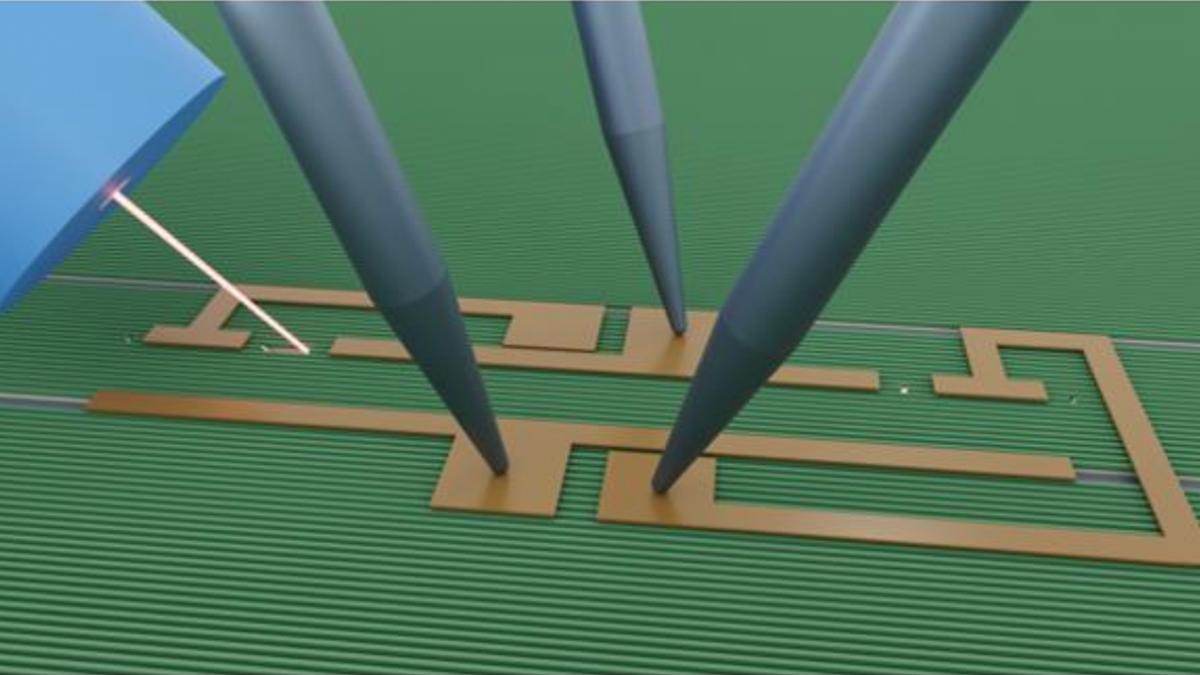
Components of a Photonic Chip
A typical photonic silicon chip consists of four main components:
- Laser (light source) – generates photons.
- Waveguides – guide photons, like wires guide electrons.
- Modulators – encode or decode data by altering light properties like intensity, phase, or wavelength.
- Photodetectors – convert light signals into electrical signals.
How Lasers Work (Stimulated Emission)
- Laser stands for Light Amplification by Stimulated Emission of Radiation.
- In this process:
- A photon causes an excited electron to release energy and drop to a lower level.
- This releases another identical photon.
- The chain reaction creates a coherent light beam – the laser.
Why Silicon Alone Doesn’t Work
- Silicon has an indirect bandgap, so it is not efficient at emitting light.
- Materials like Gallium Arsenide (GaAs) have a direct bandgap and can emit light efficiently.
- Problem: GaAs and silicon have different crystal structures, causing defects when grown together.
- These defects make the laser less efficient by turning light energy into heat.
The Solution – 'Trench Design'
- Inspired by a 2007 AmberWave Systems study.
- Researchers:
- Created deep trenches in the silicon wafer.
- Filled trenches with silicon dioxide (an insulator).
- Deposited GaAs at the trench bottom so defects remained trapped and didn’t affect the laser.
- Grew defect-free GaAs above the trench.
- Added three thin layers of Indium Gallium Arsenide (InGaAs) to act as the laser.
- InGaAs is GaAs with 20% gallium replaced with indium for better light emission.
- Covered with Indium Gallium Phosphide for protection.
- Electrical contacts were added to power the laser.
Key Data and Results
- 300 functional lasers were grown on a single 300-mm silicon wafer.
- 300 mm is the industry-standard wafer size.
- Laser emitted light at a wavelength of 1,020 nm.
- Suitable for short-distance communication between chips.
- Threshold current to power the laser: 5 mA (same as an LED in a computer mouse).
- Laser output: approximately 1 milliwatt (mW).
- Continuous operation:
- Worked for 500 hours at room temperature (25°C).
- Efficiency dropped at 55°C.
- Other optical chips have worked up to 120°C, so further stability improvements are needed.
Significance of the Breakthrough
- First monolithic laser diode successfully grown on a 300-mm silicon wafer.
- This approach:
- Solves the long-standing issue of integrating lasers with chips.
- Can lead to faster computing, lower energy consumption, and reduced costs.
- Especially beneficial for data centres, AI systems, and green computing.
- The process is scalable, efficient, and can be used with existing chip-making facilities.

From Caliphate to Corridor: Prospects for US-Gulf cooperation

US Lifting Sanctions on Syria – A Major Foreign Policy Shift

Tsarap Chu Conservation Reserve : India’s largest conservation reserve comes up in Spiti Valley
Karol Bagh Metro Pillar No. 112, Above Domino's, 22B, First Floor, New Delhi - 110060
Copyright © 2024-2026 ENSURE IAS. All rights reserved.