- Courses
- GS Full Course 1 Year
- GS Full Course 2 Year
- GS Full Course 3 Year
- GS Full Course Till Selection
- Answer Alpha: Mains 2025 Mentorship
- MEP (Mains Enrichment Programme) Data, Facts
- Essay Target – 150+ Marks
- Online Program
- GS Recorded Course
- Polity
- Geography
- Economy
- Ancient, Medieval and Art & Culture AMAC
- Modern India, Post Independence & World History
- Environment
- Governance
- Science & Technology
- International Relations and Internal Security
- Disaster Management
- Ethics
- NCERT Current Affairs
- Indian Society and Social Issue
- NCERT- Science and Technology
- NCERT - Geography
- NCERT - Ancient History
- NCERT- World History
- NCERT Modern History
- CSAT
- 5 LAYERED ARJUNA Mentorship
- Public Administration Optional
- ABOUT US
- OUR TOPPERS
- TEST SERIES
- FREE STUDY MATERIAL
- VIDEOS
- CONTACT US
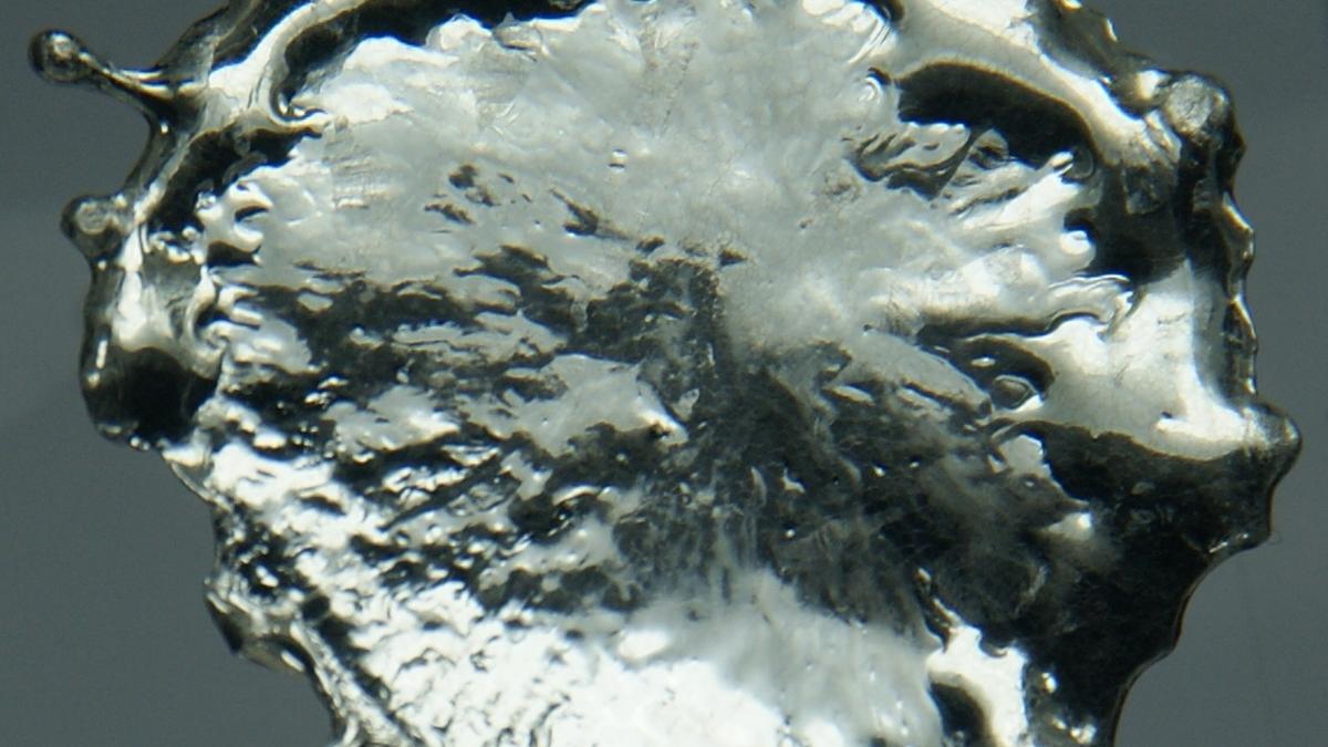
Scientists Make Strange 2d Metals Sought for Future Technologies
Scientists Make Strange 2d Metals Sought for Future Technologies
Significance: GS III; Science and Tech; Emerging Technologies;
Why in the News?
A team of researchers from top Chinese scientific institutions has reported a major breakthrough in the creation of atomically thin 2D metal sheets like bismuth, gallium, indium, tin, and lead using a high-pressure sandwich method.
- This could lead to next-generation quantum and electronic technologies, including topological insulators.
Why did scientists make strange 2D metals?
- Scientific Interest was majorly associated with the metals like Bismuth, Tin, and Lead in 2D form which were studied for their electrical, magnetic, and quantum properties.
- The study is necessary because their special properties make them useful for Quantum Computing, Sensors, and Advanced electronics.
- Featurestically, the 2D metals are only one or two atoms thick, so electrons can move in just two dimensions (hence they are called 2D metals). Due to this, they behave as if they don’t have mass, for example, giving rise to properties not seen in other materials.
|
What was the exact process?
Key Properties of MoS₂:
How is the layering done?
|
What are the technologies involved in this Research?
- Quantum Dots: They are man-made nanoscale crystals celebrated for their unique optical and electronic properties. They can transport electrons and emit diverse colors when exposed to UV light.
- Quantum Confinement: In this process, the electrons in 2D metals were restricted to specific energy levels, similar to how they behave in atoms.
- Link to 2D Metals: In 2D metals, electrons are confined in two dimensions, changing conductivity, magnetism, and optical behaviour.
What are the key challenges in making 2D Metals?
- Scalability and Large-Area Synthesis: Producing high-quality, uniform 2D metal films over large areas is difficult, limiting industrial applications.
- Thickness and Layer Control: Achieving precise control over the number of layers and uniform thickness is technically challenging but essential for device performance.
- Defects and Contamination: High defect densities and contamination (e.g., from transfer processes or precursors) can degrade the properties and reliability of 2D metals.
- Integration and Interface Quality: Creating clean, well-controlled interfaces between 2D metals and other materials is challenging, affecting device fabrication and performance.
|
What is the present progress of India in this field?
|
Way Forward: India is actively pursuing 2D materials research with strong scientific proposals and government interest, but actual large-scale progress depends on timely funding and moving from deliberation to implementation, especially as global competition intensifies.
|
PYQ Relevance Mains: Q. How is science interwoven deeply with our lives? What are the striking changes in agriculture triggered by science-based technologies? (UPSC CSE 2020)
Prelims Graphene is frequently in the news recently. What is its importance?(UPSC 2012) 1. It is a two-dimensional material and has good electrical conductivity. 2. It is one of the thinnest but strongest materials tested so far. 3. It is entirely made of silicon and has high optical transparency. 4. It can be used as ‘conducting electrodes’ required for touch screens, LCDs and organic LEDs. Options: (a) 1 and 2 only (b) 3 and 4 only (c) 1, 2 and 4 only (d) 1, 2, 3 and 4 |

|
Also Read |
|
| Public Administration Optional | |
| UPSC Monthly Magazine | Question Answer Practice For UPSC |

PLACES IN NEWS 2nd JULY 2025
10 Years of Digital India Scheme

Digital Transformation in Women and Child Development
Karol Bagh Metro Pillar No. 112, Above Domino's, 22B, First Floor, New Delhi - 110060
Very Important Instruction For Any Issue, Student Must Produce His/Her Fee Receipt. Without Fee Receipt, It Will Not Be Possible To Track Your Details. If You Have Been Given Any Special Consideration, You Must Keep That In Writing And Produce In Case Of Conflict.
Copyright © 2024-2026 ENSURE IAS. All rights reserved.